Deployable wafer devices
Flat sheets that snap into stable 3D shapes, scaled down to the chip
How far down in scale can a flat sheet be programmed to deploy into a prescribed, self-supporting 3D surface? Our earlier project on bistable auxetic surface structures established the principle at benchtop scale with laser-cut rubber sheets. This project carries the same principle to the micron scale, where standard wafer fabrication produces free-standing 3D shells.
The principle: bistable auxetic cells
The sheet is tiled with bistable auxetic cells. Each cell expands biaxially under tension (its Poisson's ratio is negative) by an amount set by its geometry, and it has two stable states separated by an energy barrier, so it snaps open and holds its expanded state with no applied force. Prescribing a spatially varying expansion across the sheet introduces an in-plane metric that cannot stay flat; the sheet buckles into a determined curved shape, and because every cell latches, the deployed surface supports itself. The cell library, the mechanics of a single cell, and the benchtop prototypes are described in the bistable auxetic surface structures project.
Designing the flat pattern for one specific shape
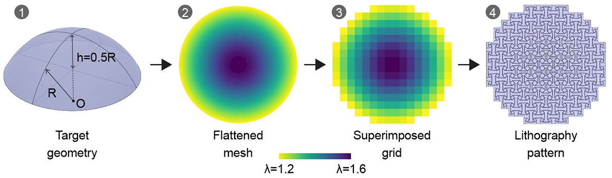
Targeting a particular surface is an inverse problem. We flatten the target 3D surface to the plane with a conformal map, which gives, at every point, the local areal scaling (the conformal factor) needed to recover the 3D embedding. From the precomputed library we then assign, at each location, the cell whose snapped-open expansion matches the required growth, choosing the stiffest, most repeatable candidate where several qualify. Tiling these spatially graded cells yields a single flat layout whose only compatible deployed state is the intended shape.
Scaling it down to the wafer
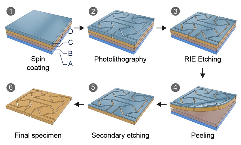
The same principle, carried to the micron scale, lets standard semiconductor processing produce 3D shells. Lithographic fabrication is extraordinarily precise but intrinsically planar, which is a real limitation for curved sensors, conformal antennas, micro-optics, and implants meant for non-developable surfaces. Here the rotating-square unit cells are defined as slits in a thin polyimide film using the same photolithography and etch steps used for flexible electronics. The full sheet is patterned in the cleanroom in roughly two days, and a release step delaminates it from the wafer without damaging the compliant hinges and without aggressive wet chemistry.
A worked example: deploying a dome
A spherical dome is the clearest demonstration of the full pipeline. The target dome is conformally flattened, the scale-factor field is sampled on a grid, and each grid square is assigned the cell whose second equilibrium matches the local expansion, producing the lithography pattern.
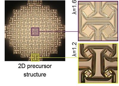
That pattern is then fabricated as a flat, spatially heterogeneous precursor on the wafer, in which cells of differing expansion appear as a visibly varying microstructure.
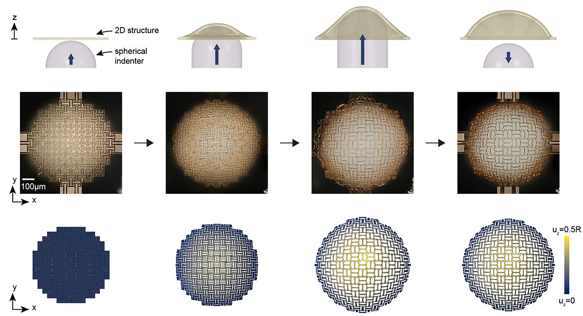
Deployment is the final manufacturing step. A spherical indenter pushes the released precursor past each cell's second equilibrium; when the indenter is withdrawn, the structure stays in its 3D shape, held by the bistability of its cells. Deployment is repeatable across samples and matches finite-element simulation, with the largest geometric deviations confined to the free rim.
Complex shapes
The method is not limited to domes. Supplying different target geometries to the design algorithm yields free-standing structures spanning a range of topologies and both positive (synclastic) and negative (anticlastic) Gaussian curvature, including a model cornea, a double dome joined by a saddle, threefold-symmetric open shapes, and an annulus. In each case the same pipeline (flatten, look up, tile, deploy) is applied unchanged; only the input surface differs.
A working optical device
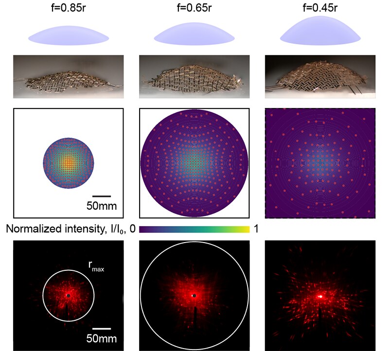
As a functional demonstration, we deploy gold-coated paraboloidal reflectors. Curvature is the whole point of a reflector, so it is a stringent test of how precisely the deployed shape matches the design. We illuminate each reflector with a collimated laser and record the reflected pattern on an imaging plane, comparing it against a ray-based geometric-optics prediction.
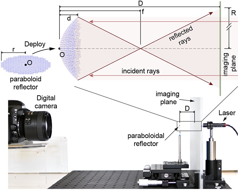
We fabricated reflectors at three focal lengths (f = 0.85r, 0.65r, 0.45r). The measured reflected patterns track the geometric-optics predictions across all three, confirming that the deployed curvature is accurate enough to function as a real optical element, produced entirely by this route.
Why it matters
By recasting shape transformation as a fabrication step, this work extends flexible electronics toward deployable electronics: antennas, conformal sensor arrays, micro-optics, and implants built with the mature, scalable toolchain of the semiconductor industry. Because the design is resolved cell by cell, the planar-to-3D map is known in advance, so functional components such as sensors can be placed at precise locations on the final curved surface.
A collaboration with the Toyota Research Institute of North America. Supported by NASA MIRO (IDEAS^2, grant 80NSSC24M0178). Fabricated at the University of Houston Nanofabrication Facility and the Shared Equipment Authority at Rice University.
Related publications
- Deployable 3D architectures from wafer-fabricated precursors. Nature Communications (2026). PDF
Press
- 2026.09 UH Parameters magazine Tian "Tim" Chen's framework uses shape-morphing surfaces and parabolic origami for deployable objects